Nippon Chemi-Con is the largest manufacturer of Aluminum Electrolytic Capacitors in the world. In addition, we also sell Silicon wafers and wafer related products as a reseller. Power semiconductors are recognized as a key device for the energy saving market and MEMS sensors are recognized as a key product for the IoT market. In order to expand and complement our existing business field of capacitors in the energy saving market and IoT market, we are supplying not only Silicon wafers, but also are offering Wafer Reclaiming services, Film Deposition services and Thermal Coupler Equipping services.
Silicon Wafer
(Prime, Monitor, Dummy)
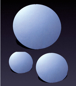
We are now supplying the range from Prime grade wafers for semiconductors to Monitor and" Dummy " grade wafers for evaluation purposes
We can supply custom made wafer s as requested.
Standard Specifications
| Wafer size | 4 inch | 5 inch | 6 inch | 8 inch | 300mm |
|---|---|---|---|---|---|
| Growth Method | CZ | CZ | CZ | CZ | MCZ |
| Diameter (mm) | 100 ± 0.2 | 125 ± 0.2 | 150 ± 0.2 | 200 ± 0.2 | 300 ± 0.2 |
| Thickness (µm) | 525 ± 25 | 625 ± 25 | 625 ± 25 | 725 ± 25 | 775 ± 25 |
| Conductivity Type | P Type | P Type | P Type | P Type | P Type |
| Crystal Orientation | <100> | <100> | <100> | <100> | <100> |
| Resistivity (Ω・cm) | 0.1 - 100 | 0.1 - 100 | 0.1 - 100 | 0.1 - 100 | 0.1 - 100 |
| Particle Size | >=0.3µm <=10pcs | >=0.3µm <=10pcs | >=0.3µm <=10pcs | >=0.2µm <=30pcs | >=0.12µm <=100pcs |
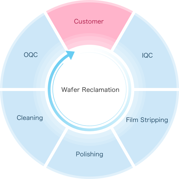
Wafer Reclamation
We offer Wafer Reclaiming services for used wafers. By using this service,
you can reduce wafer disposal.
Wafer Reclaiming Standard Specifications
| Wafer size | 6 inch | 8 inch | 300mm |
|---|---|---|---|
| Controlling particle | >=0.3µm <=10pcs | >=0.2µm <=30pcs | >=0.12µm <=100pcs |
| Controlling metal contamination | Al, Cr, Na, K, Ca, | Al, Cr, Na, K, Ca, | Al, Cr, Na, K, Ca, |
| Fe, Ni, Cu, Zn | Fe, Ni, Cu, Zn | Fe, Ni, Cu, Zn | |
| <5E10atoms/cm2 | <5E10atoms/cm2 | <5E10atoms/cm2 |
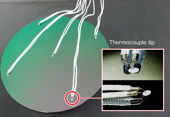
Thermal Coupler Equipping Service
It is very important for the Semiconductor manufacturing process and the LCD or OLED manufacturing process to control the surface temperature of the wafer and glass panels. We offer the service to equip a thin cable of thermal coupler to the wafer or glass panel, and also provide the measurement data of the temperature map of these products.
A difference between current service and our offered service
In the past
- Particle from fibrous insulation edge
- Easy to break strand
- Easy to get off by small contact area
Our service
- Inhibiting particle from fibrous insulation edge
- Using long life strand
- Upgrading contact strength
- High temperature response by extra fine-line thermal coupler
- We can supply a range of wafers including Silicon wafer s SiC wafers, Glass and Metal plates.
- We can provide custom made specifications as requested.
- Temperature measurement under vacuum environment is possible.
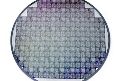
Deposited Wafer and Patterned Wafer
We also offer the service for various Film deposition and Pattern making on both 8inch and 300mm wafers.
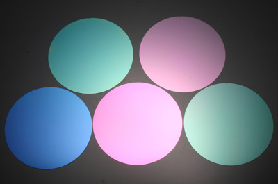
Our service characteristics of Film deposition and Pattern making
Possible Film deposition types are shown below.
| Category | Production method | Type of film |
|---|---|---|
| Oxide | Thermally oxidized film | Thin & Thick thermally oxidized film |
| LP-CVD | LP-SiO2,HTO,LP-TEOS | |
| PE-CVD | PE-SiO2,PE-TEOS,HDP etc. | |
| Spin coating | SOG | |
| Annealing | RTO | |
| Nitride | LP-CVD | LP-SiN |
| PE-CVD | PE-SiN | |
| Silicon | LP-CVD | Poly-Si,Amorphous-Si |
| Photo/Resists | Spin coating | G-line, I-line, Krf, Ar |
| Metal | Spattering | Al,Ti,Ta,Cr,Cu,W,ITO etc. |
| Coating | Ti,Ni,Au,Cu etc. | |
| CVD | W-Si |
- We can make the reticle mask for patterning by request.
- We can make 90nm size Hole patterns and Line/Space patterns for 12inch Wafers.
Contact Information
Sales Promotion GroupⅡ Sales Promotion Department Nippon Chemi-Con Corporation
5-6-4, Osaki, Shinagawa-ku, Tokyo 141-8605, Japan
- TEL
- +81-3-5436-7627